The Russian invasion of Ukraine has caused worldwide economic disruption and led to rising energy prices for oil and natural gas.
But what would be the consequences of China invading Taiwan?
We got a strong reminder of the possibility that could happen last week when China conducted military exercises around the island during the visit of US House Speaker Nancy Pelosi.
Taiwan is vulnerable. And it’s the home of TSMC, one of the world’s most advanced chipmaking companies, as well as an entire ecosystem of suppliers providing key components and advanced technology for the microelectronics manufacturing industry.
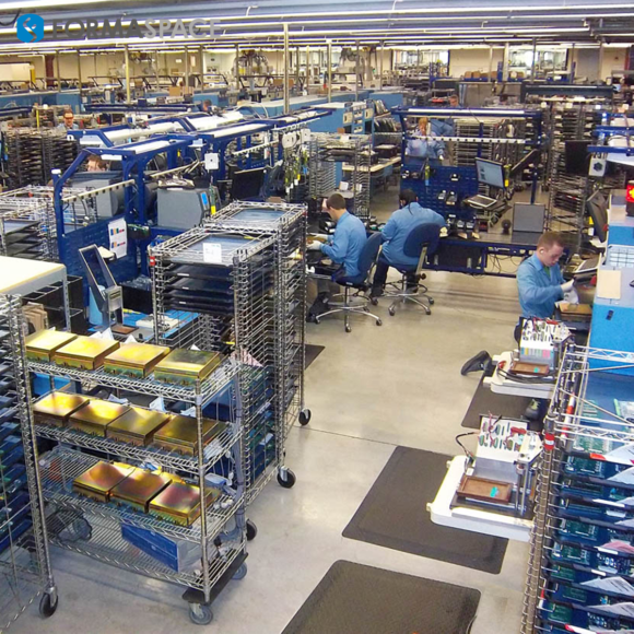
Since the start of the pandemic, chip shortages have roiled the manufacturing industry, leading to a production rollback in the auto industry alone of millions of vehicles worldwide.
A Chinese invasion of Taiwan could paralyze industries around the world (including potentially those in China) that are increasingly dependent on advanced computer chips.
The Bi-Partisan United States Chips and Science Act (CHIPS-Plus) Becomes Law
This week, President Biden signed into law the United States Chips and Science Act (also known as CHIPS-Plus), a rare bi-partisan bill that promises to invest $200 billion in the next five years to help reshore chip manufacturing operations back to the USA.
The need is great, for as we have learned all too well during the pandemic just how vulnerable our economy is to overseas producers for mission-critical parts and materials.
The bill includes increased funding and incentives for research and development, industrial chipmaking production, STEM education, and space exploration:
- $170 billion in research funding is split between the National Science Foundation and the Department of Energy to promote new technology development (including AI, quantum computing, advanced material science, and manufacturing)
- $13 billion to fund STEM education, especially in rural areas
- $39 billion in incentives for companies to build, update, or grow their US chipmaking facilities
- A new 25% tax credit for investing in new semiconductor manufacturing equipment or new manufacturing facility construction
- Funding for NASA’s moon and Mars exploration programs

Creating an Ecosystem for Leading Edge Chips Manufacturing is a Tall Order
Given the current geopolitical situation (as well as our increasing dependence on computer chips!) it’s easy to justify the need to make investments to help America to become more “chip” independent.
Unfortunately (re-)creating prowess in chipmaking technology is not easy, nor can it be accomplished quickly – so we need to set our expectations accordingly.
Experts at Intel point out it can take at least 3 years at a cost of over $10 billion to set up a new chip fabrication facility or fab.
Compounding the problem is that few manufacturers have been able to catch up with the acknowledged leader in the high-tech chip fab production field, Taiwan’s TSMC, which builds chips on a contract basis for many of the world’s leading brand name companies.
What makes the chip building industry so hard?
One explanation is that successful chip fabs need a solid support foundation – an ecosystem, in other words – that combines savvy tech leadership with multiple high-tech product and service inputs, including:
· Leadership and Finance
The chip industry is not for the faint of heart. As mentioned earlier, it takes billions of dollars to set up a chip fab and major financial investments to keep up with each successive new chip generation, driven by an expectation that (in accordance with Moore’s Law) computer chip speed/capacity will double every two years.
Leadership and vision are also key success indications. Unfortunately for the US, the Taiwanese immigrant Morris Chang (who got his degree from Stanford) felt underappreciated during his career at semiconductor maker Texas Instruments; he returned to Taiwan and founded TSMC in 1987, an incalculable loss for American technology. But it stands as a good reminder of the importance of keeping the US-educated, foreign-born scientists and engineers to stay and contribute to the American economy.
· Infinitesimal Tolerances
Under Moore’s law, chipmakers are trying to shrink the size of transistor components. Here is a chart of how the process nodes (roughly corresponding to the size of individual transistor gates) have shrunk every two-year cycle:
10 µm – 1971
6 µm – 1974
3 µm – 1977
1.5 µm – 1981
1 µm – 1984
800 nm – 1987
600 nm – 1990
350 nm – 1993
250 nm – 1996
180 nm – 1999
130 nm – 2001
90 nm – 2003
65 nm – 2005
45 nm – 2007
32 nm – 2009
22 nm – 2012
14 nm – 2014
10 nm – 2016
7 nm – 2018
5 nm – 2020
So, from 1971 to 2020, semiconductor nodes have shrunk from 10,000 nm to just 5 nm, just 0.000005% of their size in only 49 years.
Incredibly, TSMC plans to produce 3 nm chips later this year and introduce 2 nm chips in 2024, going into production in 2025-2026.
Given that the size of a typical atom ranges between 0.1 to 0.5 nanometers in diameter, it’s pretty obvious that we are talking about infinitesimal tolerances.
· Clean Rooms
We’ve written before about the challenges facing architects designing cleanrooms, but the requirements for a chip fab, especially those building 7nm and smaller semiconductor notes, are incredibly unforgiving of stray particulates.
To achieve the purification levels required by chip fab manufacturers, industrial engineers and plant managers have typically turned to multi-level production facilities that “stack” the production process vertically.
The top level, known as the interstitial, handles the air purification and temperature/humidity control.
The second level is the primary clean room, where the actual chip production takes place, where workers in bunny suits process 300mm silicon wafers, transferring the intricate chip layouts to the surface of the silicon and then sawing them into individual chips.
Underneath the cleanroom level is the “subfab” level that pipes in “lateral” supplies, such as gases and liquids for production upstairs, as well as extracting waste and exhaust gas away from the cleanroom above.
Finally, at the lowest level is the “utility” level, where the major HVAC chiller and compressor systems as well as other utilities and services.

· Water Supplies and Water Purification
Chip fabs not only require super purified air on the factory floor, they are also dependent on so-called ultrapure water (UPW), which is thousands of times cleaner than ordinary tap water – and a lot of it.
One industry source estimates a large fab may require 10 million gallons of UPW water a day. That’s a huge amount of water in a time when many regions of the US are in a drought, roughly equivalent to the daily needs of 300,000 households.
But that’s not all. To generate 10 million gallons of UPW might require somewhere between 14 and 16 million gallons of municipal water due to losses during the purification process.
The wastewater from a fab plant is not easy to process back to a useable state either.
The chipmaking manufacturing processes (including stripping, photolithography, etching, wafer back-grinding/thinning, wafer cleaning, and chemical mechanical polishing or CMP) produce large amounts of concentrated chemicals, including acids/solvents and heavy metals, and suspended particles (copper, iron, silica, etc.)
As a result, many chip manufacturers are having to add advanced wastewater treatment and recovery to their “to do” list, and some have been able to recycle as much as 98% of their water requirements.
· Ecosystem Partners for Design and Toolmaking
Even a leading fab such as TSMC cannot be successful alone – it takes a village to grow chips.
And it is this very ‘ecosystem’ that will be one of the hardest to replicate when building new fab plants in the USA.
For example, TSMC in Taiwan has a very close relationship with its partner ASML, whose machines “print” the wire circuit layout into the silicon. ASML itself (in partnership with Germany’s Zeiss) has spearheaded the development of Extreme Ultraviolet Lithography (AUM) used to create the infinitesimally small wire and gate features on today’s smallest chips.
This is just one example of the many specialized suppliers needed to support a modern chipmaking facility.
Fortunately, the US has traditionally excelled in another important aspect of the chipmaking ecosystem: circuit design (using CAD layout tools), but we will need continued investment as new technologies emerge, which is our final point.
· Investment in New Technologies
Chip foundries are at the heart of an electronics industry that is on the move, one that has maintained an astounding rate of progress year after year.
Large capital investments are a key ingredient of the secret sauce that makes this possible.
Technologies are always changing, and we can see several areas that leading chipmakers will need to place bets on to avoid being left behind.
The first is the dual impact of AI on the chip industry. AI-based tools are increasingly used to help design the latest circuit designs. And there is a growing demand for producing AI-specific chip designs to speed up machine learning and other AI-based calculations (for autonomous vehicles, for example.)
Another technology that may become more significant is the adoption of microelectromechanical systems (MEMs). In brief, these are nano-scaled mechanical devices printed directly onto the silicon chip – for example, a micro-speaker that’s “printed” rather than assembled.
A related new technology concept is Silicon Photonics, in which silicon chips are printed with small optical devices, allowing engineers to create micro optical switches and other useful devices.
Finally, advances in quantum computing, if they come to fruition, may help the industry continue to uphold Moore’s Law, but, on the other hand, if it comes to market too quickly, quantum computing-based technology could render billions of dollars of the existing fab industry’s current factory investments obsolete before their time. In this scenario, only those companies with access to quantum computing technology – and deep pockets – may survive.

Formaspace Can Help You Build Your Next Laboratory, Cleanroom, or Assembly Plant
If you can imagine it, we can build it, here at our factory headquarters in Austin, Texas.
Contact your Formaspace Design Consultant today and find out how we have been able to help Apple, Dell Computer, Google, SpaceX, and Toyota make their production facilities more efficient and productive.


